How does electricity flow through small objects?
Thursday 22nd Mar 2018, 2.57pm
Single molecules are small – really small! But what if we could harness some of their abilities to conduct and control electricity to create new electronic components? Researchers at the University of Oxford are investigating just this to find more energy efficient ways to transfer information. By looking at electricity at a small scale, we can harness the electrons’ quantum nature to revolutionise computing power and the storage of information!
How does electricity flow through large objects?
An electrical current is made up of tiny charged particles called electrons, which are quantum mechanical objects. In daily life we don’t often care about the quantum mechanical nature of our electronics because in macroscopic objects, such as lightbulbs, the electrons lose all of their information when they pass through them. When electrons enter a big piece of conducting metal from one side, they will scatter, this means that they will take billions of different pathways through the object to reach the other side.

And because the object is large, the time it takes an electron to pass through the object is long, and during this time electrons will completely forget their quantum (phase) information by the time they reach the other side.
How does electricity flow through small objects?
If electricity flows through an object that is small, such as a single molecule, we may be able to control exactly the pathway the electrons will take to cross the molecule. And if we could guide the electrons along just a few pathways the electrons will not lose their quantum (phase) information and we could potentially even use their wave-like nature to create electronic devices on the molecular scale.
How are molecular scale electronic devices made?
A team at the University of Oxford have developed a method allowing them to measure the current propagating through a single molecule. Tiny electrical contacts/wires that are small enough to contact only a single molecule are fabricated from a ribbon of graphene with a small break in it.
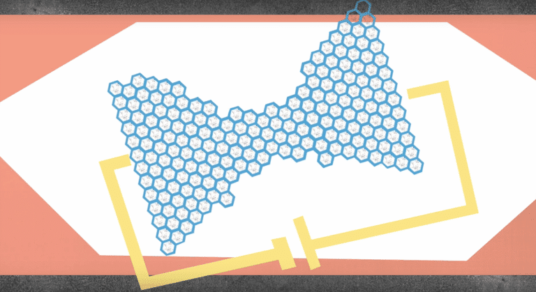
The process starts with a single layer of graphene grown by chemical vapour deposition, they then place the graphene onto a small (1x1cm) SiO2 chip with >500 pre-fabricated gold contacts. Next, electron beam lithography is used to pattern the graphene into stripes in the shape of a bowtie that cover two gold contacts each. The gold contacts can be used to pass an electrical current through the graphene and the bowtie shape is used to concentrate the current in the narrowest region. They then use fully automated feedback-controlled electroburning to form a nanometre sized gap in each device: a voltage applied to the graphene is quickly ramped up which heats up the narrowest bit of the bowtie.

This removes only a few carbon atoms by oxidation or sublimation and narrows down the bowtie which leads to an increase in electrical resistance. The resulting drop in electrical current can be detected and the voltage is rapidly ramped back to zero before the device breaks in an uncontrolled way. By repeating this step many times the graphene channel gets narrowed down until a only a few nanometre sized gap is formed. They can systematically fabricate and test large numbers of devices. Graphene is an ideal material for contacting molecules because it is very thin, chemically stable and similar to the molecules we study. Lastly, a solution of the molecule of interest is placed on the break in the graphene and hopefully a single molecule snaps into the gap allowing us to measure its electrical behaviour.

Quantum interference
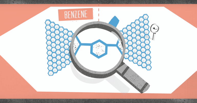
Electronic devices, when shrunk to the molecular scale, display prominent quantum effects, one of these effects is quantum interference. Quantum interference is a physical phenomenon resulting from the wave-nature of tiny particles. When, for example, entering a ring-like structure and getting offered two pathways a quantum mechanical particle will take both paths at the same time and can interfere with itself at the point where the two paths are connected again. This interference can be either constructive or destructive leading to a high or low probability for the particle to have transmitted through the ring-like structure, respectively. This phenomena has been observed in molecules such as benzene.
Electronic conduction in single-molecule devices is extremely sensitive to quantum interference, even at room temperature making this a viable quantum phenomena to exploit for developing new molecular devices.
Beyond quantum interference
One of the most exciting aspect of single molecules is that chemists can modify their functionality and scale to make vast quantities of identical devices with applications in electronics such as conductive wires, transistors, insulators and switches. Using similar graphene architectures, we can even heat one side of the molecule and measure the thermoelectric power it will produce. Therefore, in addition to computing, the technology used to measure electricity in a single molecule may also be relevant for molecular sensing, and thermoelectric resources.
The QuEEN Program
The QuEEN program is a highly interdisciplinary team of investigators from the University of Oxford (Department of Materials and Department of Chemistry) and Lancaster University (Physics Department) who are working together to develop the scientific understanding needed to exploit the quantum effects in molecular-scale electronic devices for reduced-energy computing, molecular recognition, universal memory and thermoelectric recovery of energy. Their vision is to learn how to control quantum effects in molecular electronic devices with the level of reliability necessary for applications. The QuEEN programme combines chemical synthesis, nanofabrication, measurement, and theory, and strongly relies on the interactions between these different areas of expertise.
Contact us about the following teaching resources:
KS3: What is nanoscale?
KS4: Carbon Copy
KS4: Logically Speaking
KS5: Wave Machine


